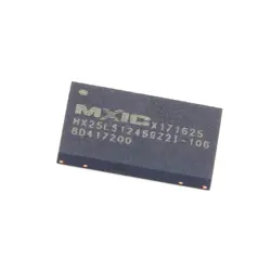
Images à titre indicatif uniquement
GD25LQ128EWIGR
+Nomenclature128MBIT NOR FLASH /1.8V /WSON8 6
-
FabricantGigadevice Semiconductor (Hong Kong) Co., Ltd
-
Pièce fabricant #GD25LQ128EWIGR
-
Package 8-WDFN Exposed Pad
-
En stock7010
365 Garantie qualité 24h/24
7*24 Garantie de service 24h/24
90-Garantie après-vente 24h/24
Garantie produit authentique
Spécifications
| Attribut | Valeur |
| Package | Tape & Reel (TR),Cut Tape (CT) |
| ProductStatus | Active |
| MemoryType | Non-Volatile |
| MemoryFormat | FLASH |
| Technology | FLASH - NOR |
| MemorySize | 128Mb (16M x 8) |
| MemoryInterface | SPI - Quad I/O |
| ClockFrequency | 120 MHz |
| WriteCycleTime-WordPage | 60µs, 2.4ms |
| AccessTime | 7 ns |
| Voltage-Supply | 1.65V ~ 2V |
| OperatingTemperature | -40°C ~ 85°C (TA) |
| MountingType | Surface Mount |
| Package/Case | 8-WDFN Exposed Pad |
Présentation
Description
Key features of the GD25LQ128EWIGR include fast read and write capabilities, low operating voltage (down to 1.65V), and a wide operating temperature range, making it suitable for various industrial and consumer electronics. It also incorporates advanced security features like block protection and OTP (One-Time Programmable) regions for data safety.
The device's compact form factor, along with its robust performance, makes it ideal for use in embedded systems, Internet of Things (IoT) devices, automotive electronics, and other applications that demand reliable non-volatile memory solutions. Additionally, it supports flexible erase and program schemes, benefiting developers with versatile data management options.
Equivalent
Features
1. Interface: Supports SPI (Serial Peripheral Interface) for communication, which allows for efficient data transfer and simplified connections with microcontrollers.
2. Voltage Range: Operates at a low voltage range of 2.7V to 3.6V, making it suitable for battery-powered applications.
3. Performance: Offers fast read speeds up to 104 MHz and supports dual/quad I/O for improved performance in data-intensive applications.
4. Data Retention: Ensures reliable data storage with a retention period of up to 20 years and an endurance of 100,000 program/erase cycles.
5. Package: Comes in an 8-pin SOP (Small Outline Package), which is compact and easy to integrate into various circuit designs.
6. Temperature Range: Designed to operate in industrial temperature ranges from -40°C to 85°C, suitable for harsh environments.
This flash memory is well-suited for consumer electronics, industrial applications, and embedded systems due to its balance of performance, capacity, and reliability.
Pinout
1. CS# (Chip Select): This pin is used to select the device. The chip is active when CS# is low.
2. DO/IO1 (Data Out/Input/Output 1): This pin is used for data output during read operations and can also serve as an input/output pin in dual or quad I/O operations.
3. WP# (Write Protect): This pin can be used to write-protect the memory array, ensuring data integrity.
4. GND (Ground): The ground reference for the power supply.
5. DI/IO0 (Data In/Input/Output 0): Used for data input during write operations and can serve as input/output in dual or quad I/O operations.
6. CLK (Clock): This pin provides the clock signal for SPI operations.
7. HOLD# (Hold): Temporarily pauses the serial communication, allowing the bus to be shared with other devices.
8. VCC (Power Supply): Provides the necessary supply voltage for the chip's operation.
The chip is used in applications requiring reliable, non-volatile storage such as in embedded systems, consumer electronics, and other digital devices.
Manufacturer
Application
1. Consumer Electronics: Used in devices like set-top boxes, smart TVs, and digital cameras for firmware storage.
2. Industrial Automation: Employed in PLCs and HMIs for configuration and data logging.
3. Networking Equipment: Utilized in routers and switches for configuration and software storage.
4. Automotive Systems: Supports infotainment systems and advanced driver-assistance systems (ADAS).
5. IoT Devices: Provides secure, non-volatile storage for sensors and connected devices.
These applications leverage the chip's fast read/write capabilities, low power consumption, and high endurance.